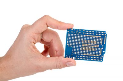
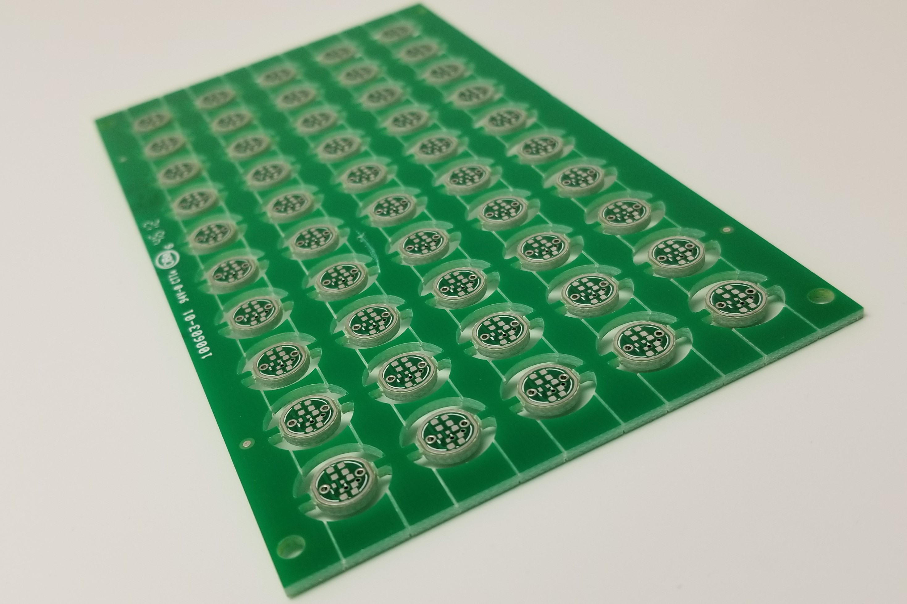
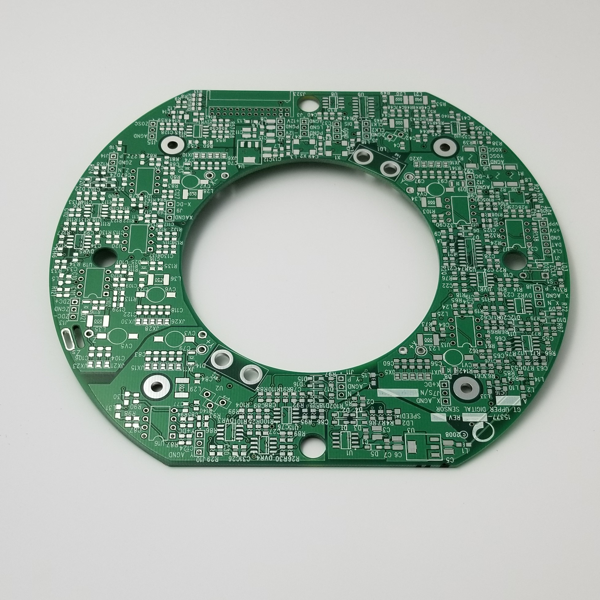
According to Circuit Digest and Printed Circuit Board Basics for Dummies, a PCB (Printed Circuit Board) is a device that provides a surface for mounting electronic components and electrical interconnections. All the electrical and electronic components are connected together on one common board with physical supports for all of the components on the base of the board. PCBs can be manufactured in a variety of shapes, sizes, and rigidity.
To better understand the basics of PCBs, we have compiled a glossary of terms. Once you are familiar with the basics of PCB terminology, get started on your PCB quote. OnBoard Circuits makes it simple, with no registration required!

In Part One of PCB Terminology, we will cover some basics about Layers, Mounting, Materials, and Finish. Stay tuned for Part Two of PCB Terminology, which will cover Stackups, Paneling and Tooling. Also, check out 4 Causes of Printed Circuit Board Failure.
PCB Terminology Part One
Bill of Materials (BOM) – a comprehensive list of all the parts required in the manufacturing process to build a specific printed circuit board. The BOM includes part numbers, manufacturer name and/or number, quantity, and description, among other pertinent information.
Gerber files – ASCII vector format files that contain specific information for each physical board layer of the PCB. Gerber files are created for each distinct physical layer of the printed circuit board and contain a series of vector coordinates to define copper traces, vias, pads, solder mask, and silkscreen images. These design files are used by PCB manufacturers to create the physical PCB.
Layers
Layer Count – PCBs can consist of one layer to multiple layers of dielectric and conductive materials. When bonded into boards, these layers carry circuits that power a variety of electronics.
Single-Layer Board – A single-layer PCB consists of one laminated and soldered layer of dielectric, conductive material.
Double-Layer Board – A double-layer circuit board consists of circuit traces on both sides of the board, connected by plated holes.
Multi-Layered Board – A multi-layer PCB is a circuit board that has more than two layers, with three or more conductive copper foil layers. Multi-layer PCBs are constructed by laminating alternating layers of prepeg and core materials under high temperature and pressure. The multiple layers are connected by plated holes.
Mounting
Through-hole technology– Through-hole technology, also spelled “thru-hole”, are holes that go completely through the boards. They can be plated (PTH) or non-plated (NPTH).
Plated Through-Hole (PTH) – Plated through-holes consist of a thin layer of copper that is plated onto the walls of the holes to provide electrical conductivity from one side of the board to the other.
Non-Plated Through-Hole (PTH) – Holes are not plated with copper for electric conductivity.
Surface-mount technology (SMT) – Surface-mount technology is a method in which electrical components are mounted directly onto the surface of a PCB.
Materials
FR4 – FR4 is a NEMA-grade composite material composed of woven fiberglass cloth with an epoxy resin binder that is flame resistant.
Rogers – Rogers designates a high-frequency board that is made with raw material produced by Rogers company. It uses a ceramic base as the high-frequency material. It has superior dielectric constant and temperature stability and is suitable for high-speed electronic design, commercial microwave, and radio frequency applications. Because of its low water absorption, it is ideal for high-humidity applications.
Aluminum – Aluminum PCBs consist of a dielectric metal base with a bonded copper circuit layer to create an effective cooling effect due to efficient heat transfer, and at the same time eliminate issues associated with managing fragile ceramics.
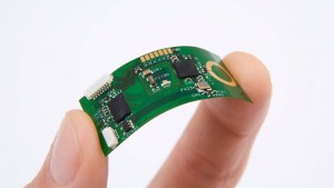
Polyimide – Polyimides are polymers consisting of imide monomers. Polyimide material is typically used in flexible and rigid-flex PCBs. Although flexible, they are high tensile strength and are resistant to warping. They are also thermally and chemically stable as well has highly durable.
Finish
Hot Air Solder Leveling (HASL) – HASL is the most common PCB surface finish. The circuit boards are immersed in a molten pot of a tin/lead alloy. Excess solder is removed by using ‘air knives’, which blow hot air across the surface of the board.
Electroless Nickel Immersion Gold (ENIG) – ENIG (electroless nickel immersion gold) is a two-layer metallic surface finish that consists of a very thin layer of gold plated over a layer of nickel. Using an electroless chemical reaction, a nickel layer is first plated on copper pads.
Electrolytic Hard Gold – Electrolytic Hard Gold is composed of a layer of gold with added hardeners for increased durability, plated over a barrier coat of nickel using an electrolytic process. Hard gold is extremely durable.
Lead-Free HASL (RoHS) – Lead-free HASL is similar to HASL, however, the solder does not contain lead, which makes this RoHS-compliant.
Stay tuned for Part Two of Printed Circuit Board Terminology! In the meantime, get started on your PCB quote today!


