In the world of modern electronics, circuit board design plays a crucial role in determining performance, reliability, and efficiency. As electronic devices become more sophisticated and compact, the need for advanced PCB solutions has grown exponentially. Multi-layer printed circuit boards (PCBs) have become the preferred choice for complex designs, offering numerous advantages over traditional single-layer and double-layer PCBs. This article explores the multi-layer PCB benefits, their applications, and why they are essential for today’s electronic innovations.
What is a Multi-Layer PCB?
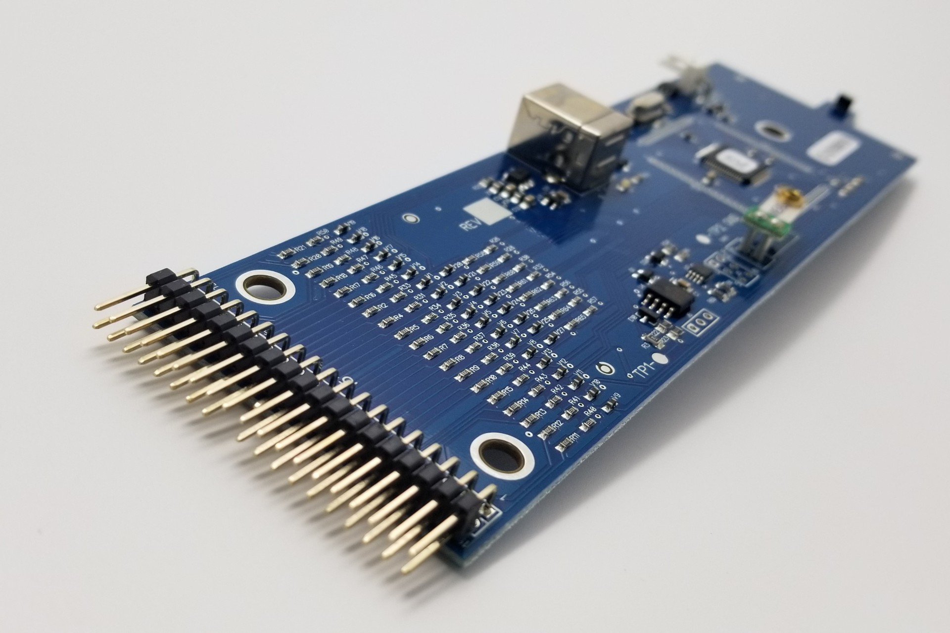
A multi-layer PCB consists of three or more layers of conductive material (usually copper) separated by insulating layers (dielectric material). These layers are laminated together under high heat and pressure to create a single, compact unit. The additional layers allow for more intricate circuit designs, improved signal integrity, and enhanced performance.
Multi-layer PCBs are widely used in industries such as telecommunications, aerospace, medical devices, automotive, and consumer electronics due to their ability to support high-speed and high-density circuit designs.
Advantages of Multi-Layer PCBs
1. Enhanced Design Flexibility
One of the primary advantages of multi-layer PCBs is their ability to accommodate complex circuit designs. With multiple layers, designers can implement more connections in a compact space without the limitations of a single-layer or double-layer PCB. This increased design flexibility allows for the integration of high-speed signals, power distribution, and ground planes in an optimized manner. Additionally, it provides the ability to separate high-speed signals from low-speed signals, minimizing interference and optimizing performance. Prototypes are an effective way to test out the design before full-scale production. Check out this article on the Benefits of Prototyping.
2. Improved Signal Integrity
Multi-layer PCBs significantly reduce electromagnetic interference (EMI) and crosstalk, leading to improved signal integrity. The ability to design dedicated ground and power planes minimizes noise and signal loss, making these PCBs ideal for high-speed communication and computing applications. Moreover, the shorter interconnects lead to lower resistance and capacitance, ensuring more stable and reliable signal transmission.
3. Higher Component Density
By incorporating multiple layers, multi-layer PCBs allow for higher component density without increasing the physical size of the board. This advantage is crucial for modern devices that require miniaturization, such as smartphones, wearables, and advanced medical equipment. The ability to stack layers enables designers to add more components, including microprocessors, memory modules, and passive components, without compromising performance.
4. Compact and Lightweight Design
Compared to multiple interconnected single-layer or double-layer PCBs, multi-layer PCBs provide a more compact and lightweight solution. This reduction in size and weight is beneficial for applications where space and weight constraints are critical, such as aerospace and portable electronics. Instead of using multiple single-layer boards connected via wires or connectors, a single multi-layer PCB reduces complexity and streamlines product design.
5. Better Power Distribution
A well-designed multi-layer PCB can efficiently distribute power across different layers, reducing voltage drops and power loss. The use of dedicated power and ground planes ensures a stable power supply to all components, improving overall performance and reliability. This optimized power distribution helps prevent power fluctuations that could negatively impact sensitive electronic circuits.
6. Increased Durability and Reliability
Multi-layer PCBs are more durable and reliable due to their robust construction. The lamination process enhances mechanical strength, reducing the risk of damage from environmental factors such as vibration, heat, and moisture. This makes them ideal for industrial and automotive applications where durability is a key requirement. The solid structure also improves thermal stability, making them more resilient to high temperatures and prolonging their lifespan.
7. Reduced Electromagnetic Interference (EMI)
One of the significant multi-layer PCB benefits is the ability to reduce EMI. By strategically placing signal layers between ground and power planes, designers can shield sensitive signals and minimize interference. This advantage is essential for applications that require precision and low-noise operation, such as medical imaging devices and aerospace systems. Effective shielding ensures that high-frequency signals remain isolated from noise-generating components, leading to cleaner signal transmission.
8. Faster Performance and Higher Speed
With shorter signal paths and improved impedance control, multi-layer PCBs facilitate faster signal transmission. This characteristic is particularly important for high-frequency applications, such as data centers, 5G networks, and advanced computing systems. The reduced parasitic capacitance and inductance contribute to lower signal delay, making multi-layer PCBs ideal for high-speed data processing and communication.
9. Ease of Manufacturing and Mass Production
Advancements in PCB manufacturing technology have made it easier and more cost-effective to produce multi-layer PCBs. Automated fabrication processes ensure high precision and consistency, allowing for mass production with minimal defects. The standardization of multi-layer PCB designs has also improved efficiency in manufacturing, reducing lead times and ensuring high-quality products.
10. Cost Efficiency in the Long Run
Although multi-layer PCBs have higher initial production costs than single-layer or double-layer PCBs, they often lead to cost savings in the long run. Their compact design reduces the need for additional connectors and wiring, lowering assembly costs. Additionally, their durability and reliability minimize maintenance and replacement costs, making them a cost-effective solution for high-performance applications.

Applications of Multi-Layer PCBs
Due to their superior performance and reliability, multi-layer PCBs are widely used in various industries. Some key applications include:
- Consumer Electronics: Smartphones, tablets, laptops, and gaming consoles utilize multi-layer PCBs for compact designs and high performance.
- Automotive Industry: Advanced driver-assistance systems (ADAS), engine control units (ECUs), and infotainment systems rely on multi-layer PCBs for enhanced functionality and durability.
- Medical Devices: MRI machines, pacemakers, and diagnostic equipment require high-precision PCBs to ensure accurate and reliable operation.
- Aerospace and Defense: Radar systems, avionics, and satellite communications benefit from the high reliability and performance of multi-layer PCBs.
- Telecommunications: High-speed networking equipment, 5G infrastructure, and fiber-optic communication systems depend on multi-layer PCBs for efficient signal transmission.
Factors to Consider When Designing Multi-Layer PCBs
To maximize the advantages of multi-layer PCBs, designers must consider several factors during the design process:
- Layer Stack-Up Design: Proper planning of the layer stack-up is essential to optimize signal integrity, minimize EMI, and ensure efficient power distribution. The choice of the number of layers and their arrangement significantly impacts performance and manufacturability.
- Material Selection: Choosing high-quality dielectric and copper materials enhances the performance and longevity of the PCB. Factors such as thermal conductivity, dielectric constant, and loss tangent must be carefully considered to meet the specific application requirements.
- Thermal Management: Effective heat dissipation techniques, such as thermal vias, heat sinks, and copper pours, help prevent overheating and improve reliability. Proper thermal management is critical for high-power applications where excessive heat could degrade performance.
- Manufacturing Constraints: Collaborating with experienced PCB manufacturers ensures that the design meets fabrication capabilities and industry standards. Design rules such as minimum trace width, via size, and layer alignment must be followed to avoid production defects.
- Cost Optimization: While multi-layer PCBs offer superior performance, balancing cost and functionality is crucial for mass production. Factors like panel utilization, via selection (through-hole, blind, or buried vias), and material choices influence the overall cost.
- Signal Integrity and Impedance Control: Ensuring controlled impedance and proper signal routing reduces signal loss and interference, which is crucial for high-speed applications. Techniques like differential pair routing and controlled dielectric spacing help maintain signal integrity.
Multi-layer PCBs can be designed using an array of PCB design software such as KiCad, Altium or CircuitMaker, among many other options.
Conclusion
The adoption of multi-layer PCBs has revolutionized the electronics industry by enabling complex, high-performance, and compact designs. The multi-layer PCB benefits, including improved signal integrity, higher component density, reduced EMI, and increased durability, make them an indispensable solution for advanced applications.
As technology continues to evolve, the demand for multi-layer PCBs will only grow, driving further innovations in electronic design and manufacturing. Whether you are developing cutting-edge consumer electronics or mission-critical aerospace systems, multi-layer PCBs provide the reliability and efficiency needed for success.
If you’re looking for high-quality multi-layer PCBs for your next project, OnBoard Circuits offers expert manufacturing solutions tailored to your needs. Contact us today to learn more about our custom PCB services! Get your free quote here!