Understanding critical design for manufacturing (DFM) principles can help to avoid costly manufacturing mistakes and unexpected production roadblocks. Designing a printed circuit board (PCB) that functions flawlessly in a simulation is a great start. However, to truly save time, money, and headaches during the fabrication process, this article will address the most common PCB design for manufacturing mistakes.
In this guide, we’ll walk through five key DFM pitfalls to avoid, based on decades of experience at OnBoard Circuits.

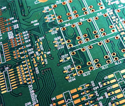
Mistake #1 – Inadequate Trace and Space Widths
Many designers focus on signal integrity but underestimate the importance of trace width and spacing for fabrication. PCB manufacturers work with minimum tolerances based on the copper weight, etching method, and board layer count. In an effort to accommodate high-density layouts, especially in compact devices, the traces can become too narrow or spacing between them too tight to be manufactured accurately.
🔍 What Can Go Wrong?
-
Traces that are too thin may not etch properly, leading to opens or poor current capacity.
-
Spacing that’s too tight can cause shorts or manufacturing defects, especially on high-density boards.
- Signal integrity issues from uneven impedance
✅ OnBoard Pro-DFM Tip:
Consult with your manufacturer’s design guidelines early on to match their trace/space capabilities. Use IPC-2221 (Generic Standard on Printed Board Design) guidelines as a baseline for trace width vs current capacity. Then, confirm the manufacturer’s minimum capabilities. Increase widths on power traces to handle higher current. Clearly communicate specifications in your fab notes.
Mistake #2 – Incorrect Pad Sizes or Via Placement
Component footprints with incorrect pad sizes, missing solder masks, or misaligned vias can result in poor soldering, tombstoning, or component shift.
🔍 What Can Go Wrong?
-
Pads that are too small can’t hold enough solder paste.
-
Overlapping pads and vias may cause unintended open circuits.
-
Blind and buried vias without proper planning can increase cost and complexity.
✅ OnBoard Pro-DFM Tip:
Use verified component libraries or consult with your manufacturer before creating custom footprints. Avoid placing vias on pads unless using via-in-pad technology and confirm the board stack-up in advance.
Mistake #3 – Lack of Clear Manufacturing Notes and Documentation
Even the best designs can fail in fabrication without proper manufacturing documentation. Incomplete or vague instructions create confusion and delay production.
🔍 What Can Go Wrong?
-
Ambiguous drill sizes or missing layer stackups
-
Unspecified finish types (ENIG, HASL, etc.)
-
Missing tolerances or test point requirements
✅ OnBoard Pro-DFM Tip:
Provide a complete Gerber file set, NC drill files, fabrication notes, and a PDF schematic. Clear callouts for controlled impedance, soldermask layers, and surface finishes will help your manufacturer build your board exactly as you intend.
Mistake #4 – Ignoring Panelization and Board Outline Considerations
Designers often submit single-board Gerbers and forget about panelization. Without a defined outline or paneling strategy, your board may need to be adjusted during the CAM (Computer-Aided Manufacturing) stage—adding time and cost.
🔍 What Can Go Wrong?
-
Unclear board dimensions or cut-outs
-
No space for tooling holes or fiducials
-
Difficulty in assembling or depanelizing boards
✅ OnBoard Pro-DFM Tip:
Work with your manufacturer to determine the optimal panel layout, especially for high-volume or automated assembly. At OnBoard Circuits, we offer panelization guidance to ensure efficient production and handling.
Mistake #5 – Neglecting Thermal and Power Distribution Planning
Thermal management is often an afterthought in early-stage PCB design, but ignoring it can cause major problems during both reflow soldering and field operation.
🔍 What Can Go Wrong?
-
Uneven copper distribution leading to warping
-
Hot spots causing component stress or failure
-
Power planes with insufficient current-carrying capacity
✅ OnBoard Pro-DFM Tip:
Use solid ground and power planes, especially on multi-layer boards, and include thermal relief pads on vias connected to copper pours. Consider adding thermal vias under hot components to dissipate heat effectively.
Final Thoughts: Collaborate Early, Save Later
Avoiding these PCB design for manufacturing mistakes isn’t just about compliance—it’s about designing a board that works both electrically and mechanically, right from the first run. An array of PCB design software such as KiCad, Altium or CircuitMaker, can be used for effective design.
At OnBoard Circuits, our engineering team works closely with clients from the first schematic through final delivery. We offer free DFM checks, fast prototyping, and quick turn PCB assembly to help you meet aggressive timelines without sacrificing quality.
📣 Ready to Streamline Your Next PCB Project?
Let us help you avoid costly mistakes and accelerate your product development.