The OEM’s Guide to PCB Prototyping: Process, Best Practices, and Technical Insights
By OnBoard Circuits, Inc.
Date: January 2026
Printed circuit board (PCB) prototyping is a foundational phase in electronic product development for OEMs. Whether developing industrial controls, medical devices, automotive systems, or IoT hardware, a systematic PCB prototype workflow dramatically reduces risk, optimizes performance, and accelerates time to market. This technical guide explores the step-by-step PCB prototyping process, key considerations for OEM engineering teams, and best practices for linking prototypes to scalable production.
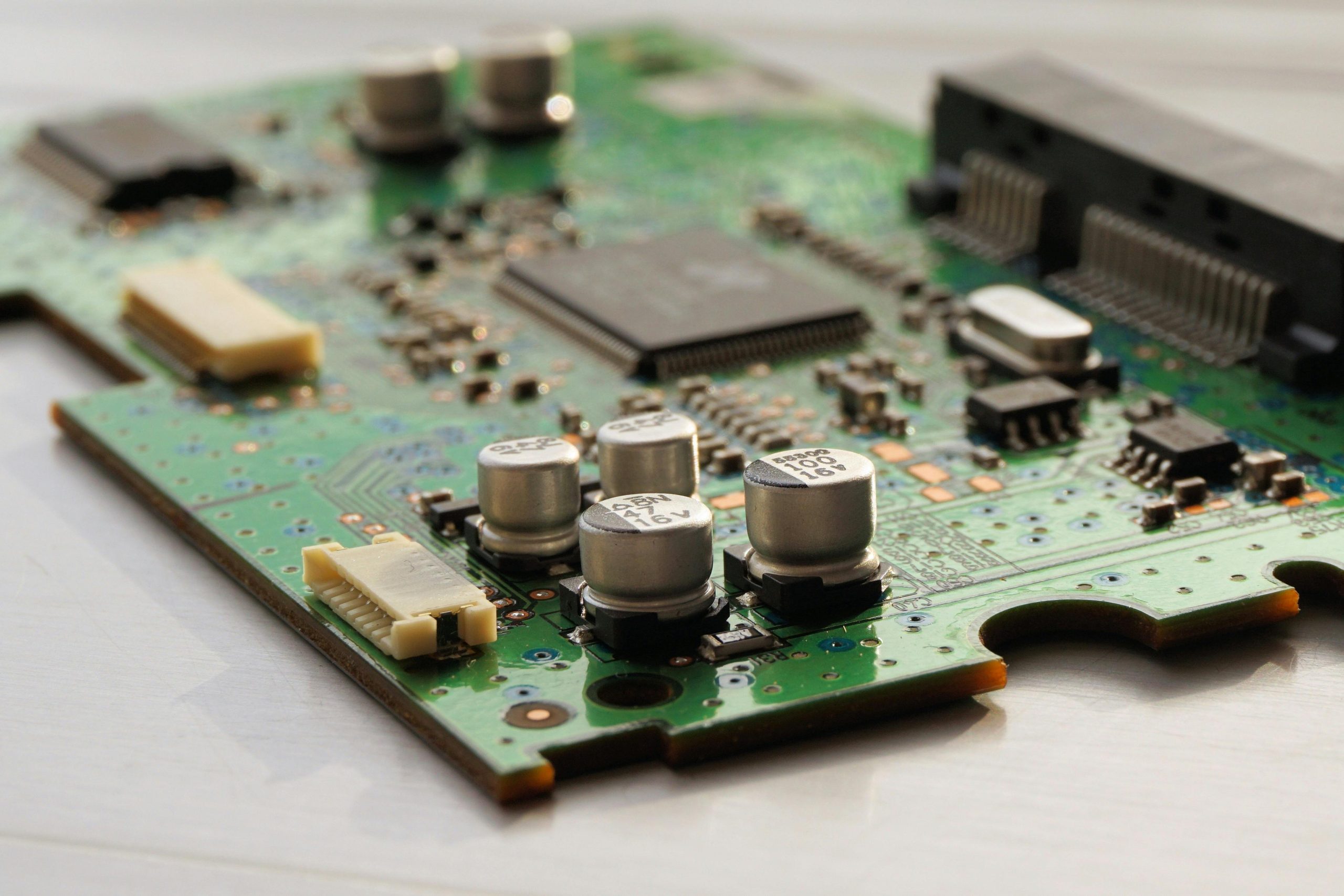
Table of Contents
1. Introduction: Why Prototyping Matters for OEMs
2. PCB Prototyping vs. Production Manufacturing
3. Step-by-Step PCB Prototyping Workflow
3.1 Requirements & Specifications
3.2 PCB Design & DRC
3.3 Gerber Generation & CAM Verification
3.4 Material Selection & Stackup
3.5 Fabrication of Bare Boards
3.6 Component Assembly
3.7 Testing, Validation & Qualification
3.8 Iteration & Refinement
4. Technical Challenges & Mitigation Strategies
5. Documentation & Traceability for OEMs
6. Diagrams to Illustrate Key Steps
7. Conclusion
1. Introduction: Why Prototyping Matters for OEMs
For OEMs, PCB prototyping is not an optional step — it’s a strategic technical checkpoint that ensures electrical design fidelity, manufacturability, and long-term reliability. A functional prototype helps uncover design flaws before committing large capital to production tooling or high-volume manufacturing. This process reduces engineering rework, avoids costly field failures, and enables parallel hardware-software integration testing well before production builds. For a deep dive into the benefits of prototyping, check out PCB Prototyping Explained: Key Benefits and Why It Matters.
2. PCB Prototyping vs. Production Manufacturing
Before diving into the workflow, it’s important to differentiate between prototyping and standard production:
| Aspect | Prototype | Production |
|---|---|---|
| Quantity | Low (1–20 units) | High (100s–100k+) |
| Turnaround | Fast (24–72 hrs) | Standard (days–weeks) |
| Tolerances | Less strict | Tightest tolerances |
| Focus | Validation & iteration | Repeatability and yield |
| Cost per unit | Higher | Lower |
Prototyping focuses on validating design intent and performance, while production prioritizes quality, consistency, and cost efficiency at scale.
3. Step-by-Step PCB Prototyping Workflow
Below is a technical breakdown of the PCB prototyping process tailored to OEM requirements.
3.1 Requirements & Specifications
Before schematic capture begins, engineering teams must formalize:
-
Functional Requirements: Power, signal types, environmental conditions
-
Standards Compliance: Automotive (AEC-Q100), medical, industrial ratings
-
Mechanical Constraints: Form factor, mounting features, and connector interfaces
-
Thermal & EMC Constraints: Heat dissipation paths, shielding needs
A comprehensive technical specification document provides early communication and serves as a baseline throughout the prototyping phase.
3.2 PCB Design & DRC
The design phase includes schematic capture and board layout using professional EDA tools like Altium Designer, Cadence, or KiCad. Critical design checks include:
-
Design Rule Check (DRC): Clearances, trace widths, impedance rules
-
Netlist Verification: Matching schematic to layout
-
Layer Stack Definition: Controlled impedance, plane layers, shielding
Failing to enforce strict DRC early leads to costly rework later.
3.3 Gerber Generation & CAM Verification
Once the board layout is complete, export:
-
Gerber files
-
Drill files
-
Netlist & BOM
Computer-Aided Manufacturing (CAM) engineers validate these outputs for consistency and manufacturability. CAM verification catches missing layers, overlapping apertures, or incorrect drill hits before fabrication.
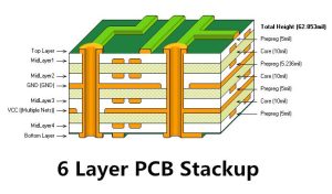
3.4 Material Selection & Stackup
Choosing the right materials impacts electrical performance and durability:
-
Substrate: FR-4 (standard); Polyimide (flex/rigid-flex); Rogers (RF)
-
Copper Weight: Affects current handling
-
Dielectric Thickness: Impacts impedance
For high-speed OEM designs, controlled impedance and matched differential pairs are essential. Decisions here affect EMC and signal integrity performance.
 (courtesy PCB Directory)
3.5 Fabrication of Bare Boards
Fabrication turns design data into physical boards:
-
Image & Etch: Creates copper traces
-
Drill & Plating: Holes for vias and through-holes
-
Solder Mask & Silkscreen: Protects and labels boards
-
Surface Finishes: ENIG, HASL, OSP based on assembly needs
Prototypes may utilize quick-turn fabrication processes, but they must mimic the intended production materials as closely as possible to yield accurate test results.
3.6 Component Assembly
Assembly places and solder parts onto the PCB:
-
SMT (Surface Mount Technology)
-
THT (Through-Hole Technology)
-
Mixed Assembly for Complex Boards
Advanced prototypes can include BGA, fine-pitch, and microvia connections to validate high-density designs.
3.7 Testing, Validation & Qualification
Prototypes must undergo rigorous technical evaluations:
-
Electrical Validation: Continuity and functional tests
-
Signal Integrity: High-frequency path characterization
-
Thermal Performance: Power cycling & thermal stress
-
EMC/ESD Pre-Compliance: Early detection of emission issues
Documented test results inform whether the design meets OEM performance criteria.
3.8 Iteration & Refinement
Testing often reveals design improvements. OEM workflows should accommodate rapid iteration:
-
Modify schematic/layout
-
Regenerate Gerbers
-
Fabricate revised prototype
-
Re-test and document
Documenting each iteration is essential for traceability and eventual production sign-off.
4. Technical Challenges & Mitigation Strategies
Even with a structured process, OEMs encounter challenges:
Tolerance Stackup Issues
Mitigation: Incorporate impedance modeling and thermal analysis before layout.
Component Availability
Mitigation: Early BOM locking and alternate part sourcing.
Complex Assembly
Mitigation: Early discussions with assembly partners and using test coupons on prototype boards.
5. Documentation & Traceability for OEMs
Robust documentation ensures that insights from prototyping carry forward into production:
-
Version Control Systems: Track design revisions
-
Test Reports: Functional and environmental data
-
Failure Analysis Logs: Root cause and corrective actions
-
Production Readiness Reports: DFM and DFA evaluation
Such documentation supports audits, compliance, and reproducibility.
6. Diagrams to Illustrate Key Steps
Below are suggested graphics that greatly improve comprehension:
-
PCB Prototyping Workflow Flowchart — Steps from design to validation
-
Layer Stackup Diagram — Typical 4-layer and 6-layer examples
-
DRC & CAM Verification Screenshot — Before vs. after errors
-
Test & Validation Matrix — What tests at each iteration stage
(These diagrams are best created by your design team or a technical illustrator.)
7. Conclusion
For OEMs developing robust, production-ready electronics, prototyping is far more than a preliminary step — it’s a strategic engineering phase that drives quality, innovation, and reliability. By following a structured prototyping workflow, enforcing design discipline, and documenting technical findings, OEM engineering teams can significantly minimize risk and streamline transitions from prototype validation to high-volume production.
To support OEM teams with advanced prototyping capabilities and world-class technical support, OnBoard Circuits, Inc. combines rapid fabrication, rigorous quality control, and industry-leading expertise to help you take your designs from concept to reality.


