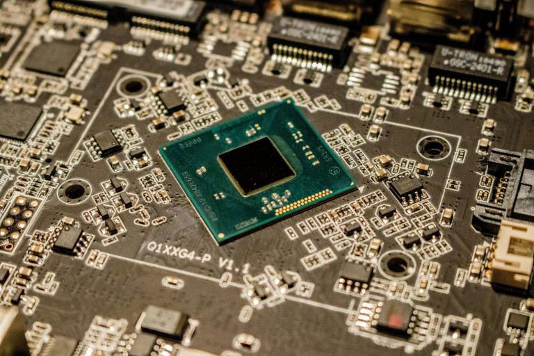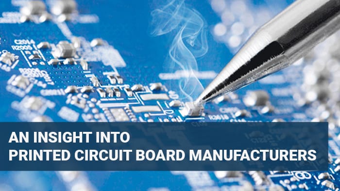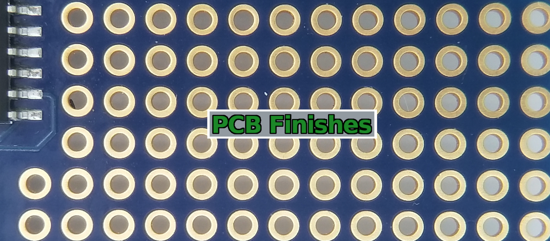
In the electronics industry, we stand on the shoulders of giants. Making electronics function reliably requires more than just electricity and magnetism theory. For example, the soldering process uses a great deal of metallurgy and chemistry to force metals to behave in ways they normally don’t. Most PCBs today use copper foil as the main conductor for its good electrical conduction and low price. But if a PCB is made with no surface finish, the ions in the air or ions in fingerprints can cause corrosion on the copper surface, which reduces the PCB solderability. Contaminants on the surface of the metal cause the solder to be repelled rather than wicking onto and completely wetting the surface to be soldered. This problem becomes exacerbated by storing products on shelves for long periods of time. To fix this, it is common to apply a surface finish to PCBs to protect the copper layer and to provide a surface that accepts solder more easily. Let’s take a look at the different options in PCB finishes commonly available and their pros and cons.
HASL (Hot Air Solder Leveling)
This is the dominating finish in the industry and comes in leaded and lead-free options with lead-free denoted as LFHASL. In this process, a PCB is dipped into a pot of molten solder, and as the PCB is slowly removed from the pot, hot air jets blow the excess solder away from the surface.
Pros:
- Mature technology and widely available
- Low Cost
- Reworkable
- Excellent shelf life
Cons:
- Leaded HASL is not ROHS compliant
- LFHASL has a higher processing temperature
- Dipping thinner PCBs in molten solder can cause thermal shock and warping especially when using a lead-free process
- The natural meniscus property of solder makes this finish less flat than other finishes
- Solder bridging can occur, not good for fine pitch components
- Can plug plated through holes.
- Not suitable for wire bonding
ENIG (Electroless Nickel Immersion Gold)
This is a two-layer metallic finish where nickel is applied directly to the copper surface, then a layer of gold is added using a displacement chemical reaction. The idea is that nickel provides a protective layer between solder and copper, and the gold layer protects the nickel from corrosion during storage.
Pros:
- Lead-free ROHS compliant
- The surface is very flat
- Good for fine pitch components, BGA, and plated through holes
- Excellent shelf life
- Suitable for aluminum wire bonding
Cons:
- More expensive than HASL and LFHASL
- Not reworkable
- Prone to “Black pad/nickel” failure
Electrolytic Nickel/Gold
This finish is divided into two camps, hard gold, and soft gold. The hard gold variety has a lower gold purity and is used for electrical contacts that will experience a lot of wear like switch contacts or “gold finger” PCB edge connectors. Soft gold has a higher purity and is often used with wire bonding.
Pros:
- ROHS compliant
- Long shelf life
- Good for contact switches and wire bonding
- Hard gold supports electrical testing
Cons:
- Expensive
- Electroplating gold fingers requires another conductive trace
- Hard gold and thicker layers of gold have poor solderability
ENEPIG (Electroless Nickel Electroless Palladium Immersion Gold)
This process has been around for a while but is being used more often recently due to the lowering cost of Palladium. This process is similar to ENIG except there is a layer of palladium between the nickel and gold layers, which further protects the nickel layer from corrosion.
Pros:
- ROHS compliant
- All pros of ENIG without black pad problems
- Better for wire bonding than ENIG
- No risk of corrosion
- Long shelf life
Cons:
- Expensive
- Newer technology, not matured
- Complex and hard to control process
Need help finding the right PCB finish for you? Call us at (888) 648-5071 or get a quote for your prototype here!