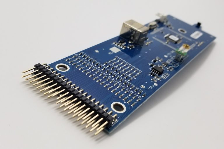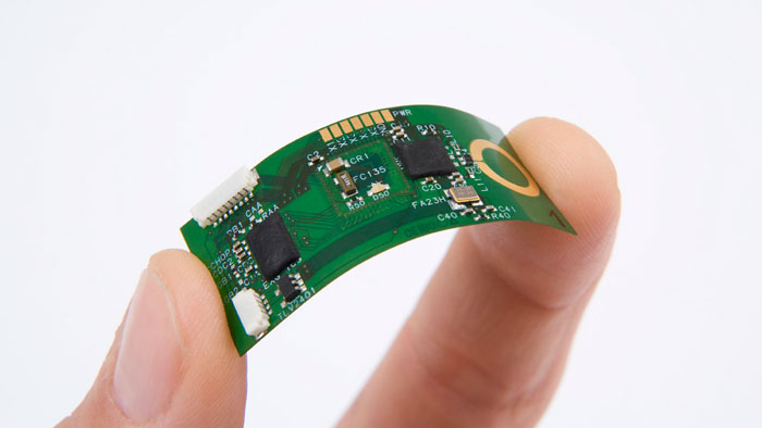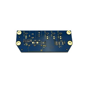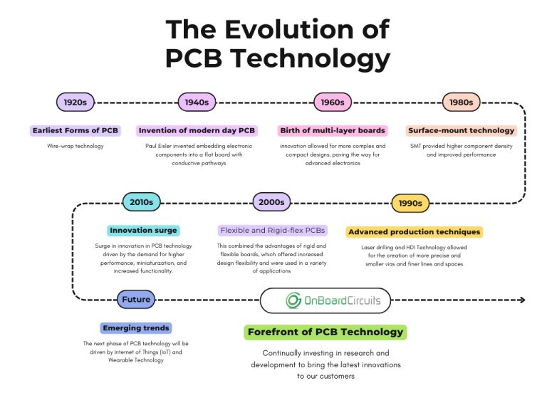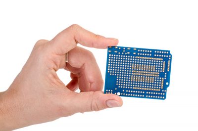
Printed circuit boards, or PCBs, are used to mechanically support and electrically connect electronic components using conductive pathways, or traces, etched from copper sheets laminated onto a non-conductive substrate. It is also referred to as printed wiring board (PWB) or etched wiring board. A PCB populated with electronic components is a printed circuit assembly (PCA), also known as a printed circuit board assembly (PCBA). PCBs are rugged, inexpensive, and can be highly reliable. They require much more layout effort and higher initial cost than either wire-wrapped or point-to-point constructed circuits, but are much cheaper and faster for high-volume production. Much of the electronics industry’s PCB design, assembly, and quality control needs are set by standards that are published by the IPC organization. Printed circuit boards can be 1 layer, 2 layered or multi-layered. The conducting layers are typically made of copper foil. The copper foil thickness is measured in ounces and can range from 0.5 oz to 4.0 oz, but are typically 1 oz. Insulating layers dielectric are typically laminated together with epoxy resin prepreg. The board is coated with a solder mask that is usually green in color. Although almost any color board can be created today. There are many different types of PCB materials available in the market. Most common are FR-1, FR-2, CEM-1, CEM-3 and FR-4. The thickness of the PCB can be 1.0mm, 1.2mm or 1.6mm. Single sided assembled printed circuit boards have all the components on only one side of the board. Boards which have components on both sides are called double sided circuit boards.
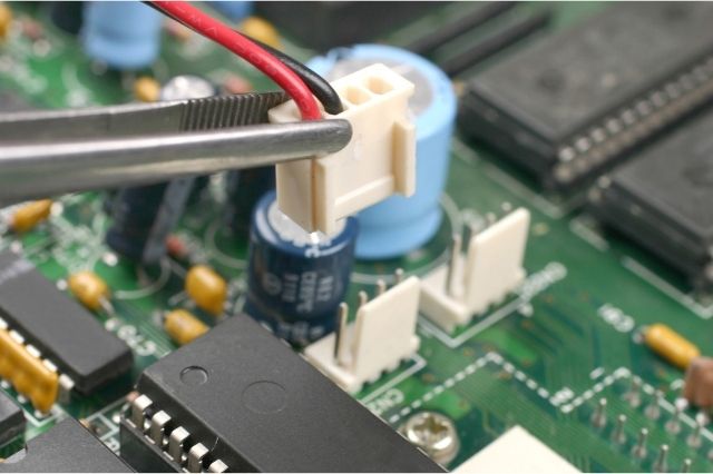
Holes are drilled on the insulator in which electronic components are fitted and these holes also work as electrical connections between different components. Components connected by through hole technology uses thin wires or leads that are pushed through small holes and soldered to connection pads in the opposite side. Components connected through surface mount technology have j-shaped legs on each component which contact circuit directly.
Before manufacturing a printed circuit board the board is designed using various layout and design CAD software. Files are created in a standard format such as a Gerber file which are given to the printed circuit board manufacturer’s engineer as the specifications to build the board. Using these specifications the engineers can fabricate the board.
PCBs made from paper reinforced phenolic resin with a bonded copper foil are less expensive. Circuits are made of copper and are coated with tin-lead layer to prevent oxidation. Insulator substrate is made by dipping or spraying epoxy resin over woven glass fiber. This is semi cured using oven and broken into large panels. These panels are placed in layers by keeping copper foil in between and subjected to high temperatures and pressure for one hour making the bond between copper foil and resin tight.
The above made substrate panel is placed in a machine for making holes in the locations that are determined during design. Generally machine is used for making holes at precise location and this machine guided through computer. Holes are made in such a way that they act as circuit using copper.
Circuit pattern is now printed on the substrate board by placing the copper in the desired pattern. The circuit is made clear by applying photo resistive material and exposing it to ultraviolet light. Then contact fingers are attached to the edge of the substrate to connect with printed circuit. Then each panel is sealed with epoxy to preventing them from damage while electronic components are mounted. Electronic components are mounted on the board at exact location on the circuit using machine. The components are then soldered to circuit. This step makes Printed Circuits boards ready to use.