Tip #1) Antipad and thermal clearances
Antipads should be 0.010 to 0.020″ larger than outer layer pads. For thermal pads, the moat should be a minimum of 0.012 ( favored 0.015) and pads should be equal to or larger than outer layer pads. Clearances for solder masks around non plated holes should be at least .005″
Tip #2) Restrictive Tolerances for the Thickness of Multilayer boards
The outcome of specifying tolerances that are very tight could be increased time and lower yields. It is recommended to call for restrictive tolerances only when they are critical to your design.
Tip #3) Minimum Text Widths Less than 0.0080” on Silkscreen Layers
Providing artwork that requires Text Widths less than 0.0080” will require extra imaging and processor steps which, in turn; will increase the cost of your project.
Tip #4) Specifying hole sizes less than 0.016″ (unless required)
Requires boards to be subjected to additional chemical processing to ensure sizing and clean-outs are complete. Along with the associated costs, these additional steps could add one full day to your processing time.
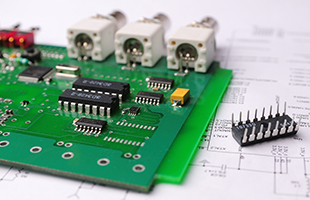
Tip #5) Providing the Choice of Capacitors
By using three holes for capacitors, you can choose between 0.1 inch and 0.2 inch spaced parts at assembly time.
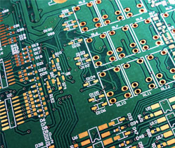
Tip #6) Use Copper Fills if Possible
Some parts are likely to get hot during usage, (motor drivers, voltage regulators.. etc.) but placing copper fills under the chips is a great way to get rid of excess heat. Another benefit of these copper plains is that they can increase performance, despite not being electrically connected to the chip or the power supply. Of course, at times you’ll need the area underneath the chip to run traces. If so, check out the next tip.
Tip #7) Use Thick enough traces for Chip’s Power Supply
At times you’ll need the area underneath the chip to run traces, and thus cannot add a copper plane (to reduce heat and improve efficiency). Instead, you can benefit from using thick enough traces for the chip’s power supply, and connect those traces to even small copper areas nearby.
Tip #8) Add a Wider Circular Pad
In many circuit boards, most of the holes don’t have traces passing closely, or at least not on the side of the board that the hole will be soldered. For the holes with free space, add a wider circular pad around the hole to provide a greater contact area during soldering. This will ensure good solder contact between the part pin and the circuit board trace. Soldering should be quicker as well, since it is easier to get the larger pad targeted with soldering tips.
Use these useful tips to help save costs on your next PCB project.