Medical electronic assemblies have unique requirements that set them apart from other types of electronic devices, such as consumer electronic products. Often, thermal management issues must be anticipated in the design, and assemblers must conform to certain quality standards such as ISO 13485. Assemblers of medical electronic products must be aware of the special requirements of such assemblies, and in particular design issues related to the printed circuit board upon which the electronic components are assembled. A working partnership between the device manufacturer and a PCB fabricator with broad knowledge of PCB design and engineering issues can greatly facilitate the successful planning and production of these specialized medical electronic circuit assemblies. This paper outlines key elements and practices of such a working relationship designed to produce high-reliability, high yield products.
In terms of unique requirements, let’s look at a couple of examples. Unlike most common consumer electronic devices, burn-in and rigorous vacuum chamber testing are vital for medical electronics and circuit board products. Burn-in involves subjecting fully functional sub-system circuit boards to different temperature cycles to ensure a full and representative simulation of the operating environment, as if the product were fully operational in a medical facility. Vacuum chamber testing puts the subsystem circuit board in a truly challenging environment, with temperature ranges from -40°C to 85°C for 24 to 48 hour test cycles and it is put into non-stop operation for periods ranging from 24 to 72 hours.
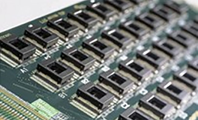
Med_Board-webThis may seem extreme, but such a circuit board could be in a remote location with temperatures over 100°F, and no air control rooms or, at the other extreme, with temperatures below room temperature or below freezing points thereby exposing the PCB to the extreme conditions. Environmental testing of this nature helps ensure 100% product reliability and can also expose latent defects. Another example of engineering considerations.
A first-OEM developed prototype of a medical circuit board product, in most instances, operates at 60% – 80% percent of designed specifications. It rarely operates at 100 percent unless large dollar amounts and extremely talented and knowledgeable engineering resources are deployed along with lots of effort. In most cases, it is just the opposite. Few OEM engineers work on a prototype and generally speaking, their main focus is on testing a few initial features that comprise the core functionality of the product. Once that is achieved, they work on ancillary functions. Therefore, much more effort must be made to start off with a better product that will stand up to rigorous testing and be reliable in the field where lives can quite often depend on the functionality of a medical electronic device. A strong working partnership between the OEM, EMS provider, and the PCB supplier is necessary. We know that to achieve high reliability goals, a sound product testing strategy must be created at the prototype stage.
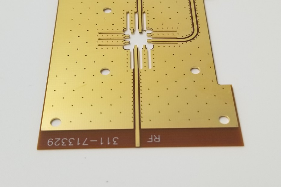
Med PCB Data Verification-web
That is when both OEM and EMS provider engineering staffs initially come together to discuss design and manufacturing objectives. In effect, the PCB prototype serves as a product R&D tool, allowing the EMS provider to increase reliability by defining and building in Design for Manufacturability (DFM) and Design for Testability (DFT) procedures within the different stages of the product development. Those include testing different environmental cycles that a circuit board undergoes to temperature and humidity. Then, there is environmental stress above and beyond regular in-circuit and functional testing. Failure rate analysis can be performed even at the prototype circuit board level to increase product yield and reliability.
Another example where OEM and PCB suppliers should work together on design is in the instance of compact PCBs with tightly spaced digital and analog circuits. In these instances, correct device placement and partitioning on the PCB takes on new meaning and requires experienced engineering staff to achieve clean and undistorted signals, at critical levels. Capabilities are key to success.
Also in the area of RF PCB Designs: correct placement and partitioning of power and ground planes is especially important for product designs that include radio frequency (RF) ICs. Hence, RF must be shielded properly and efficiently than other ICs by increasing the number of power and ground planes at the layout stage so that RF signals are sandwiched in between to keep the signal clean. RF is also shielded at assembly by using aluminum sheeting to block electromagnetic interference (EMI). In effect, aluminum shielding acts as an antenna and radiates the EMI upwards into the air and away from adversely affecting other devices.
Many medical electronic assemblies require heat management characteristics (high-power devices, RF and wireless, lighting/LED boards, etc.). It’s important that the PCB supplier has been UL certified for metal-clad PCBs with a standard dielectric, and can work with various thicknesses of aluminum and copper metal cores. Precise machining tolerance capability and high-quality fabrication services are needed for effective thermal management and long-term board reliability.
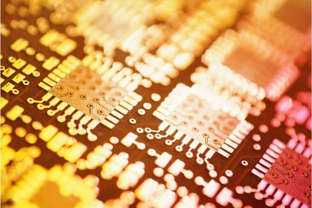
Bare Board Quality Inspection-web
Thermal management characteristics can involve everything from simple to complex multilayer constructions, and employ today’s state-of-the-art materials and configurations including the T-lam thermal lamination system, which includes T-Preg thermally conductive dielectric/ Prepreg, DSL or double-sided metal core laminate, and IMPCBs, insulated metal printed circuit boards. Other constructions include 2-layer T-lam, hybrid IMPCBs with FR-4/T-preg, multilayer metal base construction, and multilayer FR-4/T-preg hybrids.
Such thermal management PCB products dissipate heat effectively, keeping components cool which results in increased performance and life. The use of state-of-the-art materials properly designed can provide outstanding thermal performance with high dielectric strength and low capacitance and in most cases eliminate the need for fans, heat sinks, and heat spreaders.
Lastly, assemblers of medical electronics devices, particularly EMS providers (contract manufacturers), should be certified to ISO 13485. ISO 13485 is an ISO standard, published in 2003, that represents the requirements for a comprehensive management system for the design and manufacture of medical devices. While it is not yet a requirement for PCB fabricators, i.e., the supplier/manufacturer of the bare boards, it may soon be, and in any case, it is a good idea for a PCB supplier to be fully aware of the standard’s requirements and to be in compliance with them anyway.
Compliance with ISO 13485 is often seen as the first step in achieving compliance with European regulatory requirements. This standard supersedes earlier documents such as ISO 46001 and ISO 46002 (both 1997), the ISO 13485 published in 1996 and ISO 13488 (also 1996). While it remains a stand-alone document, ISO 13485 is generally harmonized with ISO 9001. A fundamental difference, however, is that ISO 9001 requires the organization to demonstrate continuous improvement, whereas ISO 13485 requires only that they demonstrate that the quality system is implemented and maintained. For any electronics manufacturer or assembler, achieving ISO 13485 certification is an important milestone, a sign of ongoing dedication to quality manufacturing.
Working together, OEM, EMS, and PCB suppliers can take on the very demanding challenge of building medical devices that must be robust and reliable with engineering considerations.