Printed Circuit Board assembly (PCBA) is the process by which raw boards and electronic components come together. While PCB design and manufacturing are critical early steps, assembly is where electronics products truly come alive.
Whether you’re developing a prototype for a startup, scaling to production, or launching a complex industrial product, understanding the PCB assembly process step by step can prevent costly mistakes and accelerate time to market.
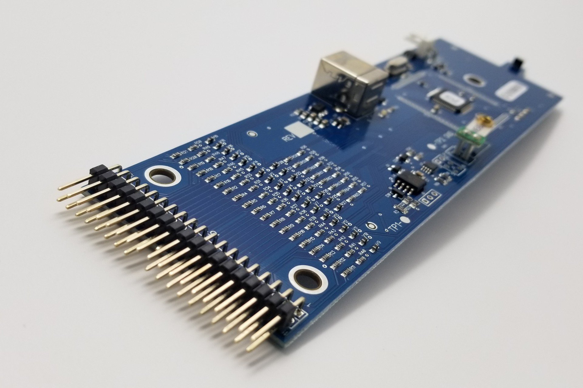
Assembly blue soldermask
What Is PCB Assembly?
PCB assembly (PCBA) is the process of attaching electronic components—such as resistors, capacitors, ICs, and connectors—onto a bare PCB. This process transforms a blank board into a fully functioning electronic circuit.
PCB assembly uses two main technologies:
-
Surface Mount Technology (SMT): Components are placed directly onto the PCB surface
-
Through-Hole Technology (THT): Component leads are inserted into drilled holes and soldered
Depending on the application, your board may require SMT, THT, or a hybrid assembly process.
Step-by-Step PCB Assembly Process
Step 1: Design File and BOM Review
Before any physical work begins, the assembly team reviews all supplied documentation to ensure clarity and manufacturability. Key files include:
-
Gerber files (copper layers, silkscreen, solder mask, outline)
-
Bill of Materials (BOM) with part numbers and descriptions
-
Pick-and-place file with X/Y coordinates
-
Assembly drawings indicating polarity, orientation, and special notes
Sample PCBA BOM
| Item | Qty | Reference Designators | Part Number (MFG) | Description | Package | Manufacturer | Substitute Allowed? |
| 1 | 10 | R1, R2, R3, R4, R5 | RC0603FR-0710KL | Resistor 10kΩ 1% 1/10W 0603 | 603 | Yageo | Yes |
| 2 | 10 | C1, C2, C3, C4, C5 | CL10B104KA8NNNC | Capacitor 0.1uF 50V X7R 0603 | 603 | Samsung | Yes |
| 3 | 1 | U1 | ATMEGA328P-AU | Microcontroller 8-bit MCU TQFP32 | TQFP-32 | Microchip | No |
| 4 | 1 | D1 | SS14 | Diode Schottky 1A 40V SMA | SMA | ON Semiconductor | Yes |
| 5 | 1 | Q1 | IRLML6344TRPBF | MOSFET N-Ch 30V 5.2A SOT-23 | SOT-23 | Infineon | Yes |
| 6 | 1 | J1 | 609-1031-ND | USB Mini-B Receptacle | USB-MiniB | Molex | No |
| 7 | 1 | Y1 | ABM3B-16.00MHZ-B2-T | Crystal 16MHz ±20ppm | HC-49/US | Abracon | Yes |
At OnBoard Circuits, we offer free DFM (Design for Manufacturing) checks to catch issues like:
-
Footprint mismatches
-
Unclear polarity indicators
-
Obsolete or mismatched parts
-
Solder mask openings that are too small
✅ Pro Tip: PCBs can be designed using an array of PCB design software such as KiCad, Altium or CircuitMaker, among many other options. Submit your files early. Pre-production review can prevent delays and costly board respins.
Step 2: Solder Paste Application
For SMT assembly, a metal stencil is used to apply solder paste (a mix of solder alloy and flux) onto each pad where a component will be mounted.
-
The stencil matches your PCB pad layout
-
Squeegees spread the paste evenly through the stencil apertures
-
Paste volume is critical—too much causes bridging; too little causes weak joints
Common solder paste types include:
-
No-clean paste (leaves minimal residue)
-
Water-soluble paste (requires cleaning)
-
Lead-free paste (for RoHS-compliant products)
✅ Pro Tip: Ensure your stencil is designed with the right thickness (usually 4–6 mils) and aperture reduction to prevent paste smearing.
Step 3: Pick and Place
Once the solder paste is applied, the PCB moves to a pick-and-place machine. These high-speed automated machines do the following:
-
Read the pick-and-place file for component coordinates
-
Use vacuum nozzles to pick components from reels or trays
-
Rotate and align components for proper orientation
-
Place each component precisely onto the solder-pasted pad
Modern machines place up to 60,000 components per hour with incredible precision (±0.05 mm).
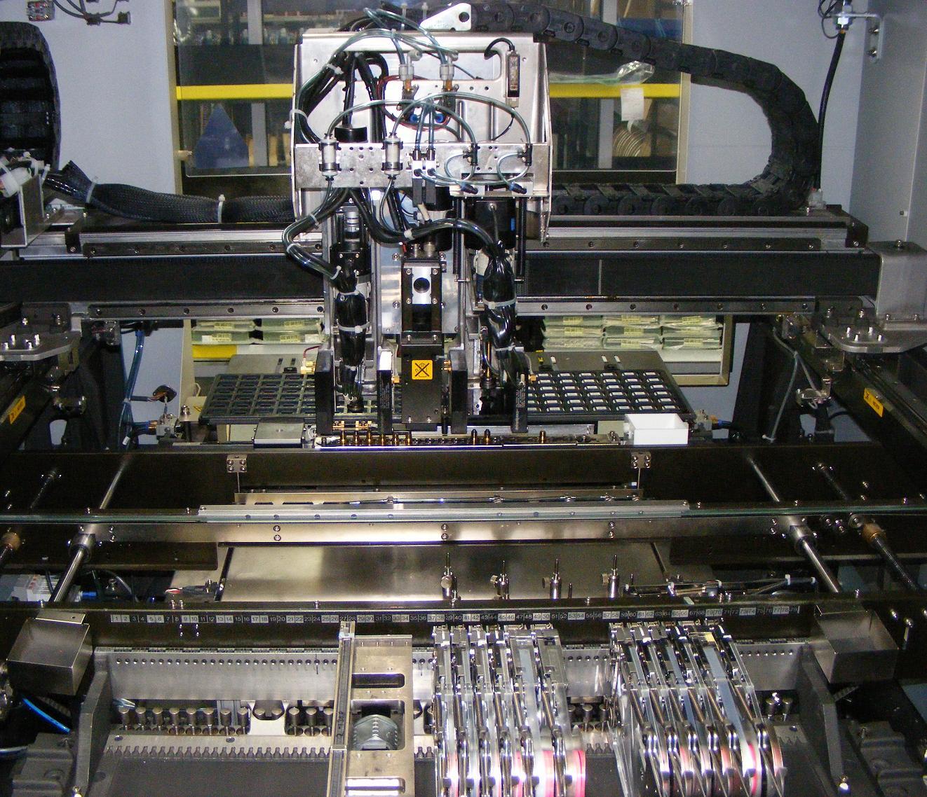
PCBA Pick and Place Machine
✅ Pro Tip: Clearly define your part orientations in the BOM and centroid files. Include fiducial marks on the board for optical alignment.
Step 4: Reflow Soldering
Once components are placed, the board goes through a reflow oven. The oven has multiple temperature zones that:
-
Preheat the board
-
Soak to remove volatiles
-
Reflow to melt solder
-
Cool down gradually
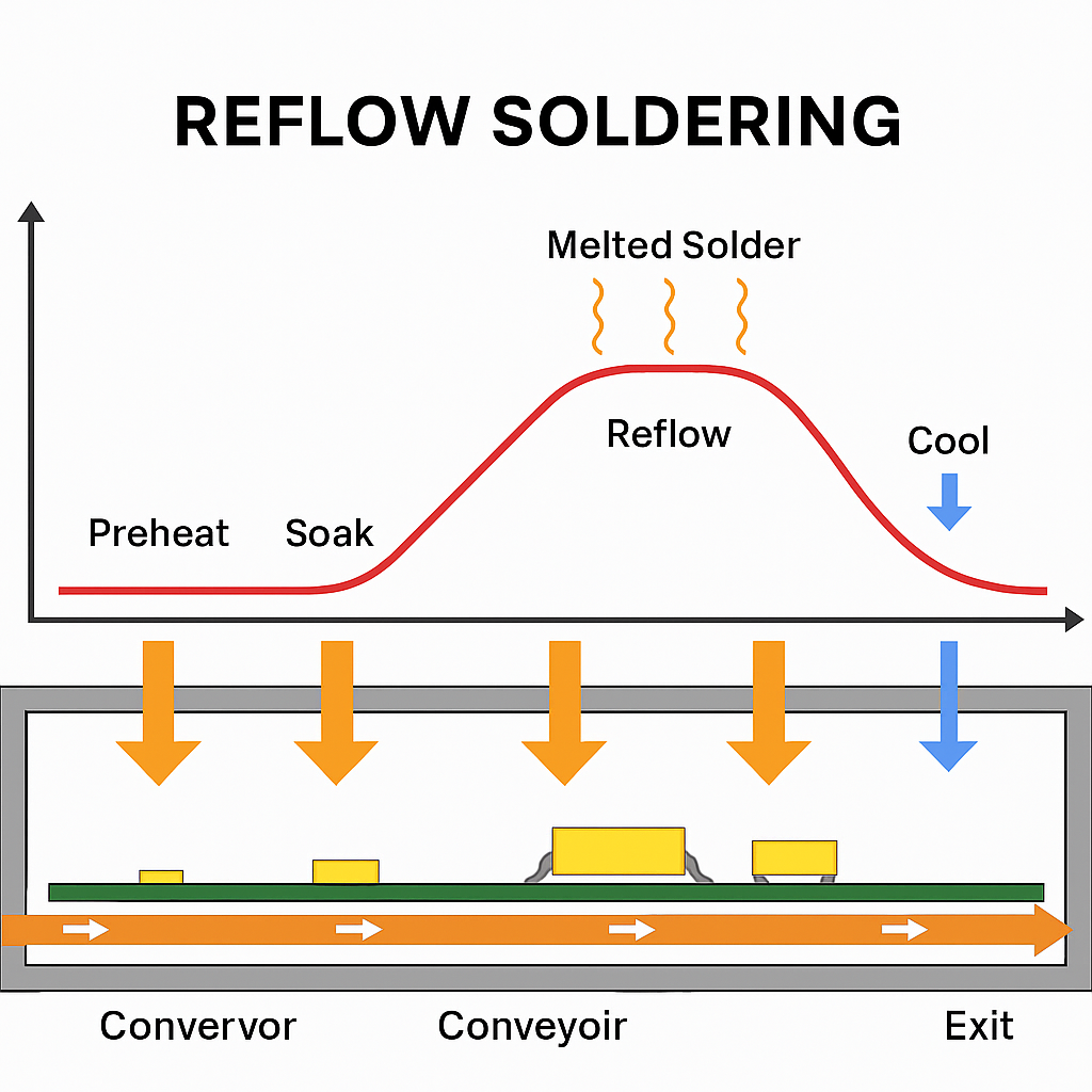
The melted solder forms solid, reliable joints between pads and component leads. The thermal profile depends on:
-
Solder paste type
-
Component sensitivity
-
PCB material (FR-4, polyimide, etc.)
✅ Pro Tip: Sensitive components like Ball Grid Arrays (BGAs) or Quad Flat No-lead (QFNs) require tight temperature control. Always share reflow profiles with your contract manufacturer for validation.
Step 5: Through-Hole Component Insertion (If Applicable)
Your board may include through-hole parts that are inserted manually or via automated insertion machines. These components include:
-
Barrel jacks
-
Connectors
-
Transformers
-
Large electrolytic capacitors
After insertion, they are soldered using:
-
Wave soldering: a conveyor passes the board over molten solder
-
Selective soldering: for targeted joints
-
Hand soldering: for low-volume or delicate jobs
✅ Pro Tip: Group through-hole parts in board design to simplify wave soldering and reduce the need for masking.
Step 6: Inspection and Quality Control
At this stage, every board goes through rigorous inspection to ensure it meets IPC standards and customer expectations.

Inspection methods include:
-
Automated Optical Inspection (AOI): Detects solder bridges, tombstoning, polarity issues, and component alignment
-
X-ray Inspection: Used for BGAs and hidden joints
-
In-circuit testing (ICT): Measures resistance, capacitance, and signal continuity
-
Functional testing: Simulates operating conditions to ensure performance
OnBoard Circuits adheres to IPC-A-610 Class II or Class III standards depending on customer needs.
✅ Pro Tip: If you require test services, provide test points, instructions, and custom fixtures during the design stage.
Step 7: Cleaning, Packaging, and Shipping
Post-inspection, the board goes through final prep:
-
Cleaning (for water-soluble flux): Removes residues that could corrode or conduct electricity
-
Labeling: Includes lot codes, date codes, and traceability marks
-
Packaging: ESD-safe bags, moisture barrier bags, foam padding, and anti-static boxes as needed
✅ Pro Tip: Specify any special labeling or packaging requirements when requesting a quote.
Additional Considerations in PCB Assembly
✔️ RoHS Compliance
If your product is sold in Europe or California, you may require lead-free (RoHS-compliant) assembly. Be sure to:
-
Choose compatible parts and solder paste
-
Label clearly on the silkscreen if needed
✔️ Assembly Types
-
Turnkey Assembly: Your contract manufacturer (CM) handles everything, including sourcing components
-
Consigned Assembly: You provide the parts
-
Partial Turnkey: A hybrid—CM sources common parts, you provide special ones
✅ Pro Tip: OnBoard Circuits supports all three models.
✔️ Lead Time and Turnaround
Typical PCBA turnaround times vary:
-
Prototype runs: 4 weeks, can be done sooner if requested
-
Production runs: 4-6 weeks, expedited services available depending on BOM complexity
We offer quick-turn PCB assembly with no Minimum Order Quantity (MOQ), perfect for R&D and low-volume builds.
Common Mistakes to Avoid in PCB Assembly
-
Inaccurate BOMs (missing values, alternate part numbers)
-
No polarity indicators on silkscreen
-
Parts not available in reels/tape (can delay pick-and-place)
-
Omitting fiducials (for alignment)
-
Mixing leaded and lead-free parts in RoHS builds
✅ Pro Tip: Prevent delays by getting a DFM consultation early in the process.
Frequently Asked Questions (FAQ)
1. What is the difference between PCB manufacturing and PCB assembly?
-
PCB manufacturing creates the physical board from copper-clad laminate.
-
PCB assembly adds and solders the components to make it functional.
2. Can OnBoard Circuits source components for me?
Yes! We offer full turnkey service, component sourcing, and part substitutions if needed.
3. What files do I need to submit for assembly?
-
Gerber files (RS-274X)
-
BOM (Excel preferred)
-
Pick-and-place file
-
Assembly drawing (PDF)
-
Special instructions (if any)
4. Do you offer functional testing?
Yes—include test procedures and fixtures if required.
✅ Pro Tip: At OnBoard Circuits, we specialize in high-quality PCB manufacturing and assembly, offering fast turnaround and DFM support at every stage.
Why Choose OnBoard Circuits for PCB Assembly?
When precision, speed, and support matter, OnBoard Circuits delivers. With decades of experience, we support everything from one-off prototypes to production-level builds with equal attention and care.
We’re proud to offer:
-
Quick-turn PCB assembly in as little as 3 days
-
Free DFM checks and design feedback
-
In-house quality control and inspection
-
Full support for SMT, THT, and hybrid builds
-
RoHS and leaded solder options
Let’s Build Something Together
👉 Click here to request a Free Assembly Quote Today
📞 Or call us at 888-648-5071 to talk to an expert about your next build.
🔗 Related Blog Posts:
What to Look for in a High-Quality PCB Manufacturer


