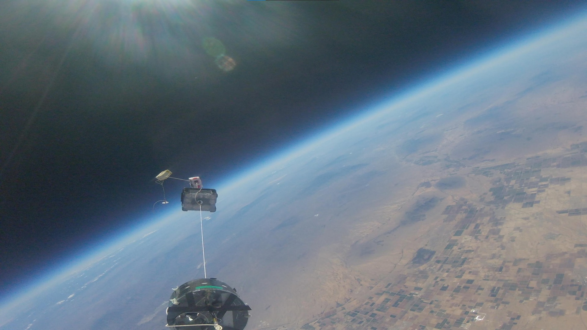
Building an electronic device can be a difficult task and especially daunting for those that are less experienced in the field like students. A local organization, the Arizona Space Grant Consortium is giving students an opportunity to gain some serious experience through their high altitude weather balloon program. Their program operates by setting two dates per year for launching hydrogen-filled balloons, grouping students into teams, then designing an atmospheric or engineering experiment that will be attached to the balloon and sent into the sky. To ensure their success, the teams must wisely consider what environment their end product will have to endure.
How’s the weather up there?
The course of the flight consists of the launch, flight, pop at up to 100,000ft, and a parachute landing, with a total of around 3 hour flight time. Over the course of the flight, the balloon travels through a thick atmosphere at up to 50mph and as cold as -50F, then through a vacuum swinging back past 100F, then the balloon pops and shakes the payload at up to 5Gs. The payload then falls through the same atmospheric layers slowing itself with a parachute and finally landing on the ground with a softer force than felt at the pop.
Roadmap through rough terrain
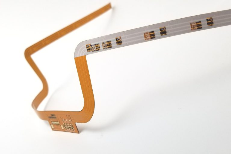
Given these conditions, a systems designer is wise to optimize their design by minimizing the payload’s weight since the propellant required for lift increases exponentially with overall payload weight. They might choose smaller wires and connectors over larger heavier ones, they might put extra effort into their PCB layout to minimize the resulting size or choose a 2 or more layer PCB as opposed to a single layer that requires more PCB weight. The strong forces make a sturdy set of mounting holes essential as improper fastening and mechanical stability can cause PCB cracking. A flexible PCB can be a great choice for this situation since the substrate is lighter in weight than rigid designs and its flexibility offers vibration tolerance. Vacuum can have a tendency to increase the static discharge from exposed electronic contacts, this problem can be mitigated with the use of a conformal coating, creating a protective insulating layer, stopping shorts from occurring. Every component of the PCB must be carefully chosen such that all of them have an operating temperature range that can accommodate the extreme temperatures, but also the designer must consider how much each active device is self-heating and choose components that have a lower self-heating rate. Component weight, temperature stability, and lower self-heating can make smaller surface mount components a great choice. Because of the expected temperature extremes, it can be a good choice to test the prototype on a burn-in board to detect any possible faults that may occur later due to heat or cold.
Vigilant design
A designer must remain diligent and aware of the trade-offs and unexpected consequences of an otherwise good design choice. For example, an MS5607 altimeter might at first seem like a great choice for its good price and ease of use, but its datasheet and application note claims direct light can cause variation in how it reads pressure, which depending on the desired operation of the system, that may or may not be a good choice.
Whether the device has an intended operating environment is in the deep sea, edge of space, or a PLC at a factory requiring high reliability and uptime, careful care should be taken to understand the environmental conditions with which the system needs to operate.
Have a question about our PCB specs? We are glad to help! Give us a call today at (888) 648-5071 or get a PCB quote here!